


By EMCrafts
Supplier Info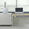
Product Type:
Metrology & Handling
Application:
Scanning Electron Microscope
Product Description:
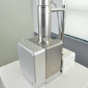
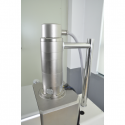
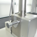
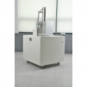
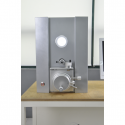
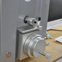
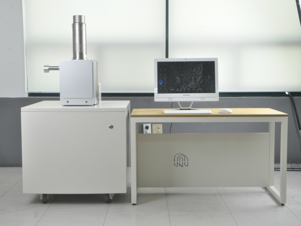
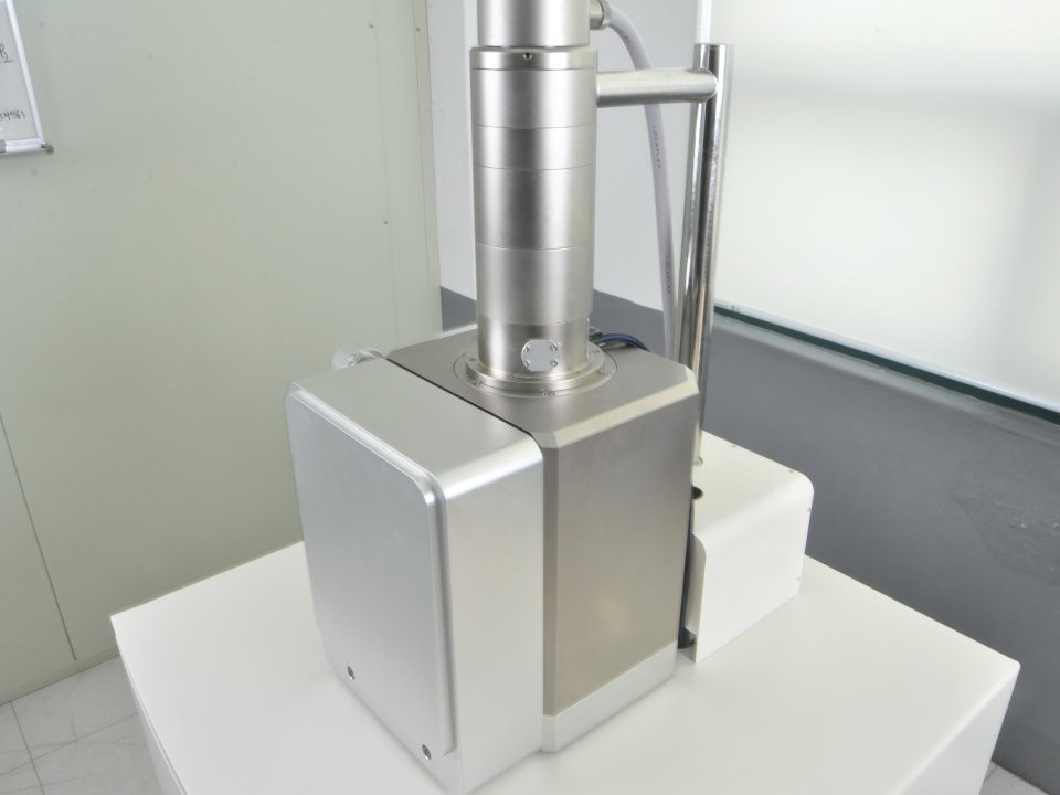
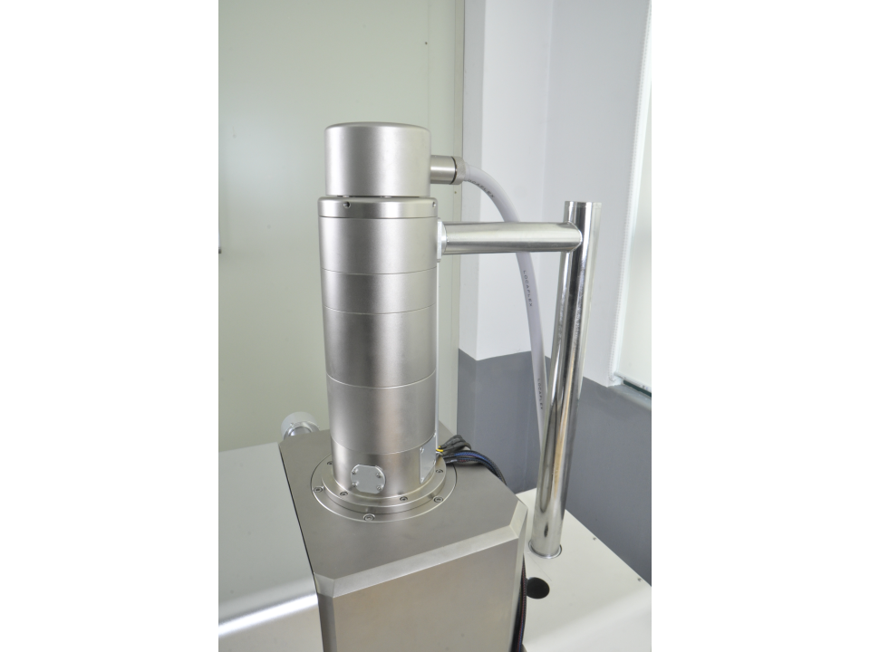
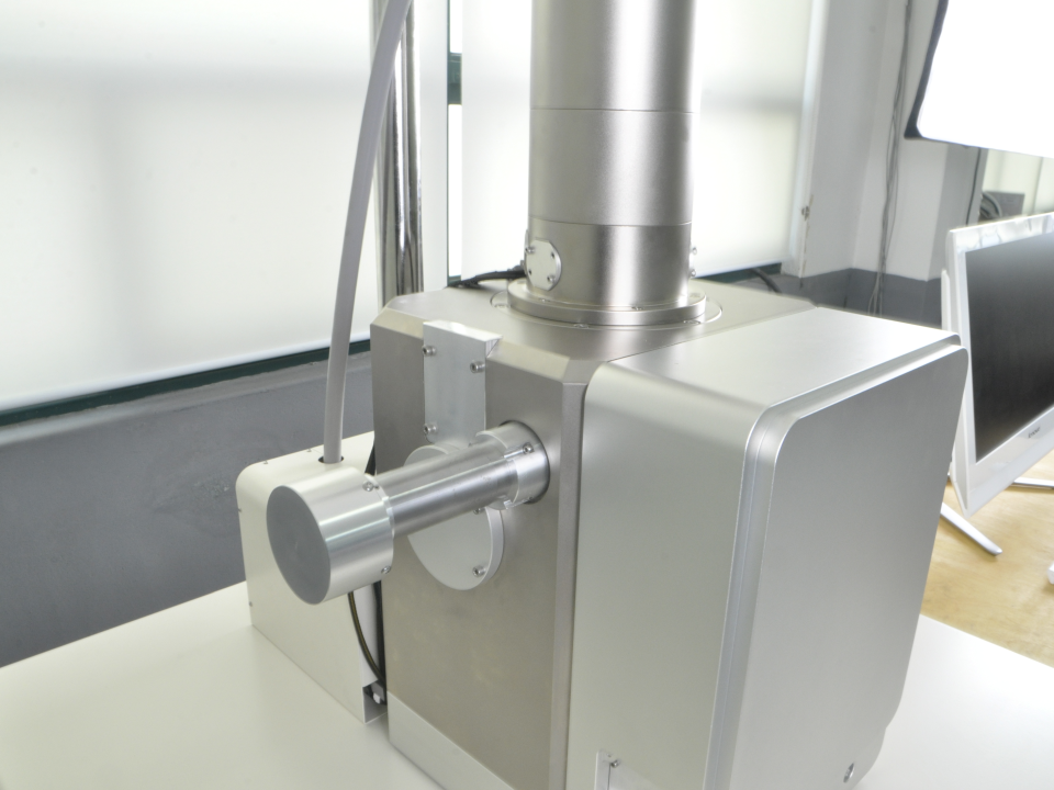
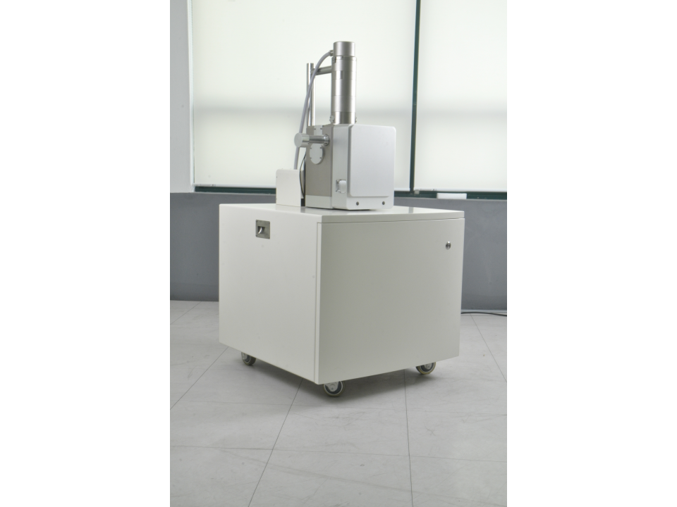
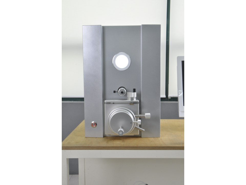
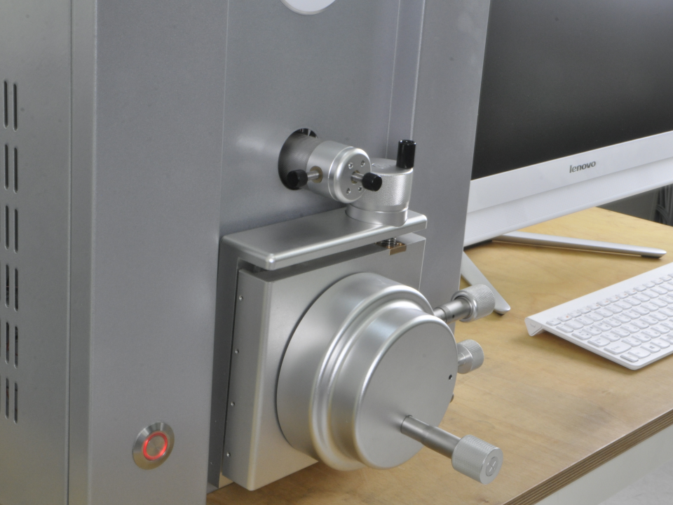
EMCrafts Veritas Series:
Big Chamber Scanning Electron Microscope
- 5-Axis motorized stage
- 200V ~ 30kV
- X 10 ~ X 300,000 Magnification
- Resolution: 3.0nm (SE Image at 30kV)
- Auto Brightness & Contrast, Auto Focus, Auto Gun Alignment, Auto Saturation, Auto Filament, Bias
- for Specimen with width 210mm and height 65mm
- up to 2kg specimen (metals, wafer, compact disc, PCB)
- analyze specimen within 3 minutes after loading
For Details on VERITAS-Series, please contact us using our contact form.
There are currently no downloads available.
There are currently no videos available.
Semiconductor / Mems Area
SEM is widely used across various fields to produce unprecedented images of the microscopic and nanometric world.
Our family of SEM models are widely-used in research fields and industry applications such as semiconductor, flat-panel display, and nanotechnology labs .
- Quality control of electronics circuits and semiconductor parts
- Observation of microstructure of Secondary cell, CNT (Carbon Nano Tube), Solar Cell, Wafer, Bonding Wire, LED, Nano tech
Life Sciences
As an entirely new advanced imaging tool for bioscience research, SEM had contributed much to advancing the field of life science.
SEM is frequently used in observing not only the structure of living organisms
but also tissue models as well as nano-particle analysis of drugs .
- Micron-scale insect anatomy
- Detailed images of surface structures of plants
- Nano-particle analysis of drug delivery
- Red blood cell and white blood cell segmentation
Green Energy
SEM has become an indispensable solution for natural resource companies to analyze, measure, extract and refine relevant features in rocks, minerals and man-made materials.
Our model of SEM is used in numerous applications, such as in the mining and geoscience industries.